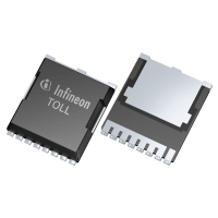
There are various ways to classify MOSFETs (Metal Oxide Semiconductor Field Effect Transistors), and the following analysis will be conducted from different dimensions to present their classification system in a logically clear manner:

1、 Classified by conductive channel type
N-channel MOSFET (NMOS)
Carrier: Using electrons as conductive carriers, they usually have lower on resistance and faster switching speed due to their higher mobility than holes.
Application scenarios: Widely used in high-frequency switching power supplies, motor drives, and digital circuits that require fast response.
P-channel MOSFET (PMOS)
Carrier: Using holes as conductive carriers, the driving circuit design is relatively simple, but the conduction resistance is high.
Application scenarios: Commonly used in CMOS logic circuits, low dropout linear regulators (LDOs), and certain analog signal processing scenarios.
2、 Classified by gate drive characteristics
Enhanced MOSFET (E-MOSFET)
Working principle: The gate voltage needs to exceed the threshold voltage (VGS (th)) to form a conductive channel.
characteristic:
N-channel enhanced type: When a positive voltage is applied to the gate, it conducts, and after conduction, the current increases with the increase of gate voltage.
P-channel enhancement type: When a negative voltage is applied to the gate, it conducts, and after conduction, the current increases as the gate voltage decreases.
Application scenario: Used as a switching element for power conversion, motor control, and digital circuits.
Depleted MOSFET (D-MOSFET)
Working principle: When the gate voltage is zero, there is already a conductive channel, and the channel width can be controlled by adjusting the gate voltage.
characteristic:
N-channel depletion type: Applying negative voltage to the gate can narrow the channel and even clamp off the current; Positive voltage enhances current.
P-channel depletion type: Applying a positive voltage to the gate can narrow the channel, while a negative voltage enhances the current.
Application scenario: Suitable for scenarios that require default conduction, such as constant current source circuits or certain analog circuits.
3、 Classified by manufacturing process and structure
Flat MOSFET
Structure: Traditional planar structure forms channels through lateral diffusion.
Characteristics: Mature technology, low cost, but large parasitic capacitance, limiting high-frequency performance.
Application scenario: In the general field of medium and low voltage, such as consumer electronics power management.
Super junction MOSFET (SJ MOSFET)
Structure: Optimize the electric field distribution by alternately arranging P-type and N-type regions in the vertical direction.
Features: Significantly reduces on resistance, improves voltage resistance and energy efficiency, and reduces switching losses.
Application scenarios: High frequency switching power supplies, inverters, and electric vehicle charging modules.
Shielded Gate MOSFET (SGT MOSFET)
Structure: Adopting a split gate design to reduce gate charge and on resistance.
Features: Faster switching speed, higher efficiency, suitable for high-frequency applications.
Application scenarios: In the field of medium and low voltage, such as fast charging adapters and LED drivers.
Silicon carbide MOSFET (SiC MOSFET)
Material: Use silicon carbide (SiC) semiconductor material.
Features: High voltage resistance, low on resistance, wide operating temperature range, suitable for high temperature and high voltage scenarios.
Application scenarios: New energy vehicle charging stations, photovoltaic inverters, and industrial motor drives.
Gallium Nitride MOSFET (GaN MOSFET)
Material: Gallium Nitride (GaN) semiconductor material is used.
Features: Extremely high electron mobility, switching speed up to MHz level, and extremely low power consumption.
Application scenarios: 5G communication power supply, satellite communication, and high-frequency RF power amplifier.
4、 Classified by voltage and power level
Low voltage MOSFET (LV MOSFET)
Voltage withstand range: usually below 100V.
Features: Low on resistance, fast switching speed, suitable for high-frequency switching and low dropout linear regulators (LDOs).
Medium Voltage MOSFET (MV MOSFET)
Voltage withstand range: 100V to 600V.
Features: Balanced withstand voltage and on resistance, suitable for industrial power supplies, motor drives, and consumer electronics.
High voltage MOSFET (HV MOSFET)
Voltage withstand range: above 600V.
Features: High voltage resistance, suitable for high-voltage power management, smart grids, and electric vehicle charging systems.
5、 Classified by packaging form
Plug-in packaging
Types: such as dual in-line package (DIP), transistor outer package (TO).
Features: The pins pass through the PCB board, and the soldering is reliable, but the volume is relatively large and gradually replaced by surface mount.
Surface mount packaging
Types: such as D-PAK, SOT-23, QFN.
Features: Small size, suitable for automated surface mount production, widely used in portable devices and consumer electronics.
The classification system of MOSFETs covers multiple dimensions from materials, structures to application scenarios. In actual selection, factors such as voltage resistance, conduction resistance, switching speed, packaging size, and cost need to be comprehensively considered. For example, in electric vehicle charging modules, super junction MOSFETs or silicon carbide MOSFETs are preferred due to their high-frequency and high-efficiency characteristics; In consumer electronics power management, planar MOSFETs or shielded gate MOSFETs are widely used due to their cost-effectiveness.
