The continuous miniaturization of fuse volume is an inevitable result of the development of the electronics industry, which contains a synergistic evolution of materials science and precision manufacturing. From the early tubular glass packaging to the current rice grain sized patch structure, this transformation is mainly driven by three core forces:
Firstly, the breakthrough of nanoscale alloy materials has revolutionized the circuit breaker mechanism. Researchers use metal powder metallurgy technology to create micrometer sized composite particles of silver, copper, and rare earth elements, which are then stacked into porous structures using 3D printing technology. This design reduces the effective conductive cross-sectional area per unit volume by 75%, while achieving precise melting through rapid oxidation of particle gaps during current overload. The latest carbon nanotube reinforced alloy developed by a Japanese laboratory can even carry 20A current in a volume of 0.5mm ³, and its melting response speed is 300% faster than traditional materials.
Secondly, microelectronic packaging technology has spurred a structural revolution. Using the photolithography etching process in semiconductor manufacturing, a tree like fractal conductive network is formed inside the fuse. This biomimetic structure exhibits low impedance characteristics during normal operation, and when abnormal currents occur, the fractal end produces a chain like melting effect due to a sharp increase in current density. The patented technology of a German company shows that the fuse consistency of this type of structure is improved by 90% compared to linear design, but the volume is reduced to 1/8 of the original product.
Thirdly, the precise control of thermodynamic models enables spatial compression. Through finite element simulation, engineers constructed asymmetric heat dissipation channels inside the miniature fuse. In an 80 ℃ working environment, this design enables precise control of the thermal accumulation area within a range of 0.01mm ³ around the melting point. UL laboratory tests in the United States have shown that the 0402 packaged fuse (1.0 × 0.5mm) using this technology has a breaking capacity 1.5 times that of traditional 5 × 20mm glass tubes.
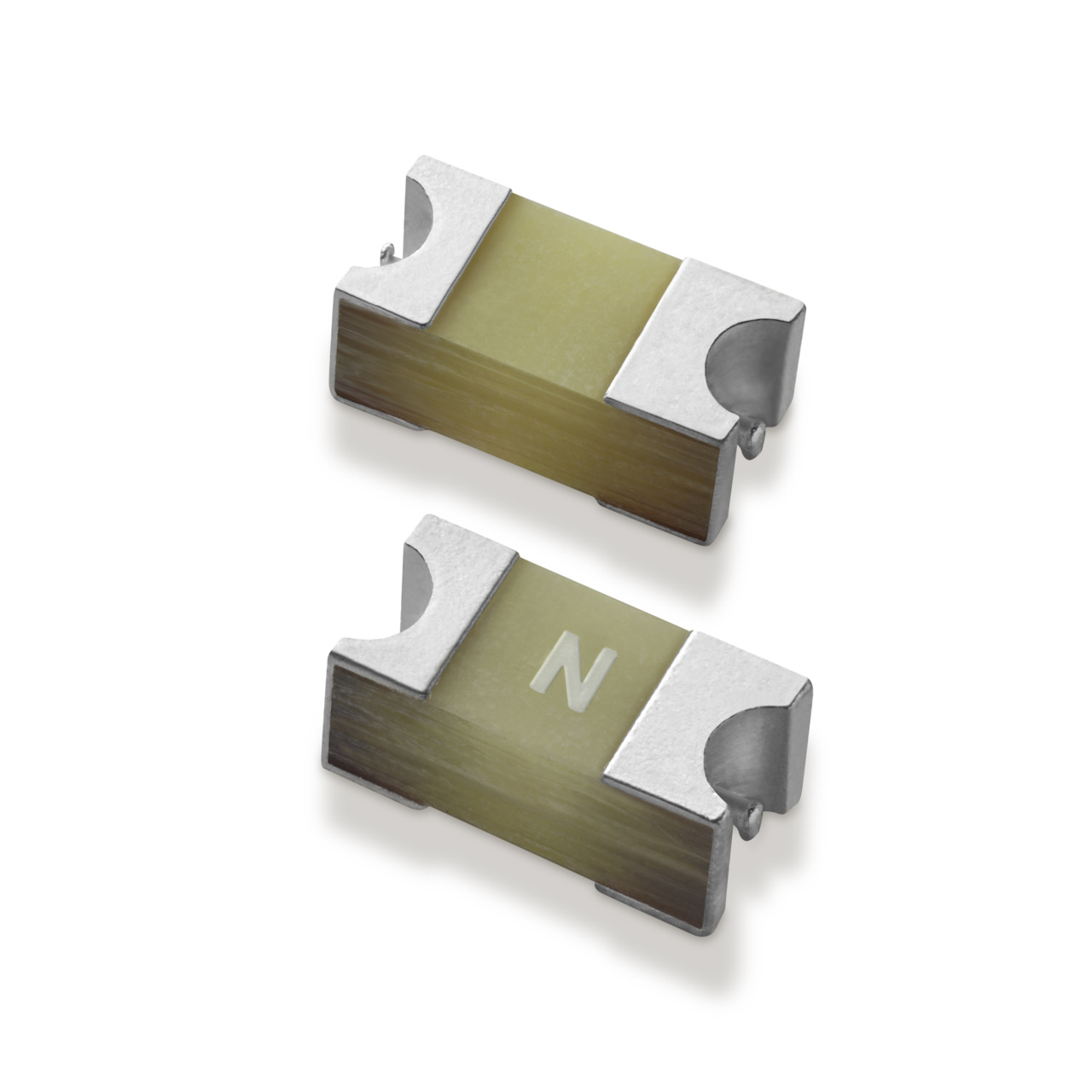
This miniaturization process is reshaping the paradigm of circuit protection. The 01005 specification fuse (0.4 × 0.2mm) used on a certain smartphone motherboard has a built-in fault self diagnosis chip that can predict the risk of melting through impedance changes. This intelligent fuse has reduced its volume by 97% compared to products ten years ago, but it has achieved preventive protection function. In the future, with the combination of two-dimensional materials and MEMS technology, molecular level circuit protection devices may break through physical limits and safeguard electrical safety at a more microscopic scale.